
Current Issue
Evaluation of DC-DC Converters Using MATLAB Simulink
Eze Cornelius C.1, Obe Chinedu T.2, Ugbe Oluchi C.3Madueme Victory4Oti Stephen Ejiofor5,
Department of Electrical Engineering, University of Nigeria,Nsukka,, Enugu State, Nigeria.
1email: cornelius.eze.241975@unn.edu.ng2email: chinedu.obe@unn.edu.ng, 3email: oluchi.ugbe@unn.edu.ng,4email: victory.madueme@unn.edu.ng, 5email: stephen.oti@unn.edu.ng.
ABSTRACT
This study explores the design, modeling, and simulation of three important DC-DC converter topologies—buck-boost, Ćuk, and SEPIC—employing MATLAB Simulink as a robust simulation environment. Each converter is thoroughly modeled to assess its voltage regulation performance under varying operational conditions. MATLAB Simulink serves as an advanced platform for analyzing dynamic system behaviors and optimizing critical design parameters, including duty cycle, switching frequency, and passive filter components. The comparative analysis focuses on output voltage stability, conversion efficiency, and transient response characteristics. The simulation parameters, while not exhaustive, are carefully selected to exhibit the operational principles and performance trade-offs inherent to each topology. The findings elucidate the different advantages and limitations of the buck-boost, Ćuk, and SEPIC converters, providing valuable insights for selecting the optimal topology tailored to specific power electronic applications, such as renewable energy systems, electric vehicles, and portable electronics. This research contributes to the broader understanding of DC-DC converter design and its practical implications in modern power management systems.
Keywords:Buck-boost converter, Conversion efficiency, Ćuk converter, DC-DC converters, Dynamic system behaviors, MATLAB Simulink, Power electronic applications, SEPIC converter, Switching frequency, Voltage regulation.
1. INTRODUCTIONDC-DC converters, which adjust the voltage of direct current (DC) from one level to another is an aspect of electrical cum electronic area that the gains cannot be ignored. Their applications in the renewable DGs include but not limited to wind turbines, wave generators, photovoltaic (PV) generators, small hydro, and fuel cells. These renewable resources have strong daily and seasonal patterns and often produce power and voltage varying with natural conditions. However, for practical exploitation and efficient use of resources, renewable generating units must be connected to the grid and especially when power electronic converters, (PECs), are deployed, particularly, as interface between wind turbine and the grid. The DC-DC Converter block represents a behavioral model of a power converter. This power converter regulates voltage on the load side. To balance input power, output power, and losses, the required amount of power is drawn from the supply side. Alternatively, the converter can support regenerative power flow from load to supply.
2.LITERATURE REVIEWThe advent of integrated circuits revolutionized electronics, enabling the rise of portable applications and industrial energy conversion devices [1-5]. DC-DC converters, which adjust the voltage of direct current (DC) from one level to another, have gained significant interest due to their efficiency in maintaining constant output voltage despite varying input levels [6-8]. These converters serve various applications by offering high conversion efficiency and stable voltage from no load to full load [7-11]. Designing controllers for such systems requires understanding their dynamics [12-14]. MATLAB, developed by MathWorks [15], offers a powerful platform for matrix manipulation, data plotting, and algorithm implementation, while Simulink enhances this with graphical simulation for dynamic and embedded systems.
In [12], the importance of steady-state conditions in DC converters was highlighted, noting that ripple magnitudes are negligible compared to steady-state values. Parameters like gain, harmonic distortion, and input/output impedances were analyzed under steady-state operation. However, time-stepping simulations to reach steady state are often impractical due to large time constants relative to the switching period. While steady-state analysis provides insights, it assumes ideal components, neglecting non-ideal characteristics such as parasitic resistances, capacitances, and non-linear effects like saturation and dead-time, which can impact performance. In this paper, we focus on the DC-DC converter model, acknowledging that simulation limitations, like the inability to account for dynamic factors such as temperature changes, may cause minor deviations from real-world performance. These differences are expected to be minimal and unlikely to affect the study’s conclusions.
3. METHODOLOGYSwitched-mode DC-DC converters temporarily store input energy and release it at a different voltage, either higher or lower, using magnetic (inductors, transformers) or electric (capacitors) storage components. This method is more power-efficient than linear voltage regulation, which wastes energy as heat.
There are different types of non-isolated DC-DC converters, each with unique circuit topologies and characteristics.3.1 Buck-Boost Converter:
This is a versatile topology that can step up or step down the input voltage, depending on the duty cycle of the switch. This topology combines elements of both buck and boost converters, making it suitable for applications with varying input voltages or when both step-up and step-down conversions are needed. They integrate a buck converter on the input side and a boost converter on the output side, utilizing a common inductor. Such converters are especially useful in battery-operated devices where maintaining a stable output voltage is crucial, even as the battery depletes.
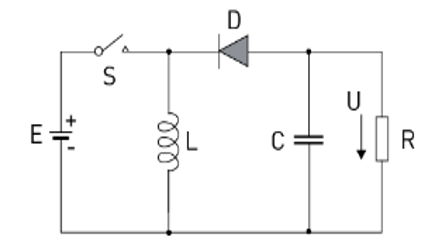
Figure 5: Diagram of a buck-boost converter
When the switch (S) is closed (ON), current flows from the input voltage source through the inductor (L), which stores energy in a magnetic field. The voltage across the inductor equals the input voltage (E), and the current through the inductor increases linearly. The diode (D) is reverse-biased during this phase, preventing current flow to the output. When the switch opens (OFF), the inductor maintains the current flow due to its stored energy, reversing its voltage polarity. This forces current through the diode to the output capacitor and load. The output voltage can be higher or lower than the input voltage, depending on the duty cycle (the ratio of ON time to total cycle time). The output voltage always has an opposite polarity to the input, which is why the buck-boost converter is also known as a voltage inverter.
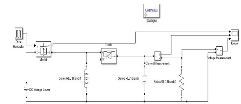
Figure 6: Circuit diagram of a buck-boost converter using MATLAB
The Duty cycle D is given as:
%%%%%%%%%%%%%%%%%%%%%%The minimum inductance of the inductor for the converter to work in continuous current mode is given by:
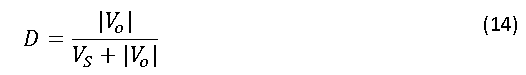
\[ D = \frac{|V_o|}{V_s + |V_o|} \tag{1} \]
\[ L_{\min} = \frac{R \times (1 - D)^2}{2 \times F_s} \tag{2} \]
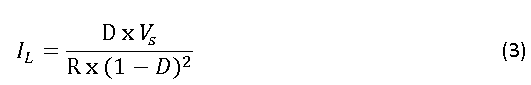
\[ i_L = \frac{D \times V_s}{R \times (1 - D)^2} \tag{3} \]
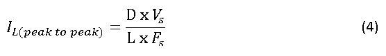
\[ i_{L(\text{peak to peak})} = \frac{D \times V_s}{L \times F_s} \tag{4} \]
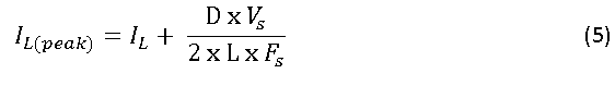
\[ i_{L(\text{peak})} = i_L + \frac{D \times V_s}{2 \times L \times F_s} \tag{5} \]
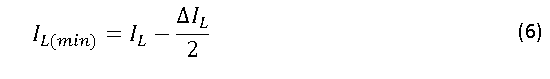
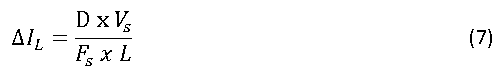
\[ i_{L(\min)} = i_L - \frac{\Delta i_L}{2} \tag{6} \]
\[ \Delta i_L = \frac{D \times V_s}{F_s \times L} \tag{7} \]
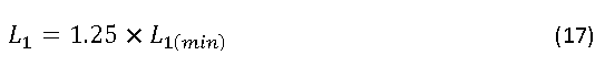
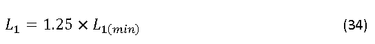
\[ L = 1.25 \times L_{\min} \tag{8} \]
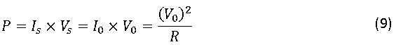
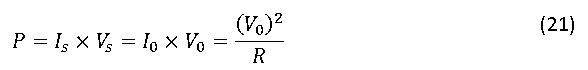
The power is given by:
\[ P = I_s \times V_s = I_o \times V_o = \frac{(V_o)^2}{R} \tag{9} \]
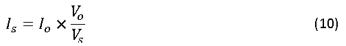
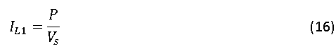
The input current \(I_s\) is given as:
\[ I_s = I_o \times \frac{V_o}{V_s} \tag{10} \]
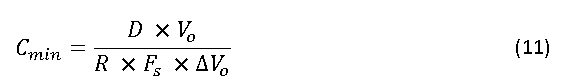
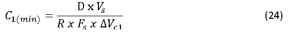
The minimum capacitance of the output capacitor is given by:
\[ C_{\min} = \frac{D \times V_o}{R \times F_s \times \Delta V_o} \tag{11} \]
Where \(\Delta V_o\) is 1% to 5% of \(V_c\).
\[ V_c = V_o \tag{12} \]
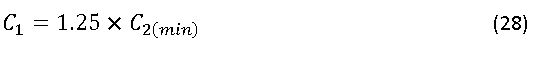
\[ C = 1.25 \times C_{\min} \tag{13} \]
%%%%%%%%%%%%%%%%%%%%%
The minimum inductance of the inductor for the converter to work in continuous current mode is given by:

The power is given by:
The input current I_s is given as:
The minimum capacitance of the output capacitor is given by:
Where ∆Vo is 1% to 5% of Vc
The Ćuk converter provides both step-up and step-down voltage conversion with low current ripple. It combines inductors and capacitors for high efficiency and improved performance. Ideal for power supplies requiring low ripple and high efficiency, such as in analog circuits, it uses a single switch and shared capacitor to transfer energy between buck and boost stages.
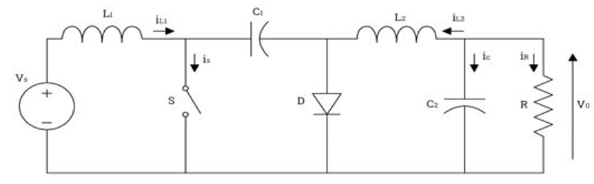
Figure 7: Diagram of a ćuk converter
When the switch (S) is closed, current flows through inductor L1, building magnetic energy and charging capacitor C1. The voltage across L1 equals the supply voltage (Vs), and the diode (D) isolates L2 and C2 from the input. When the switch opens, L1 maintains current flow due to its collapsing magnetic field, increasing its voltage above Vs, forward-biasing D. Current then flows from C1 through L2, charging C2 and supplying energy to the load. L2 builds its own magnetic field, further transferring energy to C2. The output voltage (Vo) can be higher or lower than the input, depending on the duty cycle. Like the buck-boost converter, the Ćuk converter often produces an inverted output voltage. Unlike most DC-DC converters that use inductors for energy storage, the Ćuk converter relies primarily on capacitors.
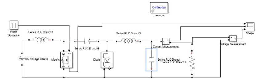
Figure 8: Circuit diagram of a Ćuk converter using MATLAB
The Duty cycle D is given as:
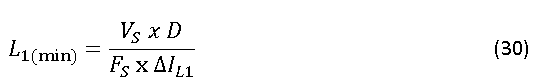
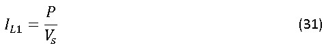
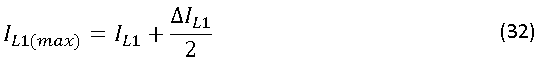
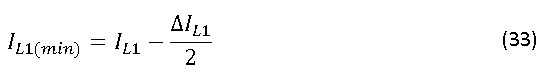
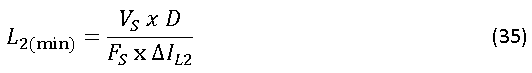
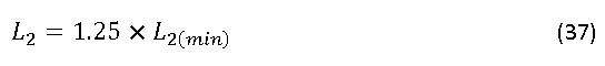
The minimum inductance of the inductors for the converter to work in continuous current mode is given by:
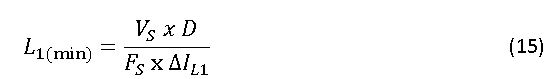
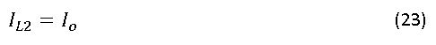
Where ∆IL1 is 20% to 40% of IL1
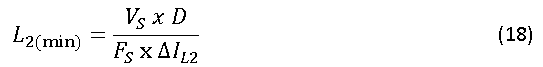
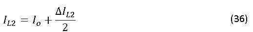
Where ∆I_L2 is 20% to 40% of IL2
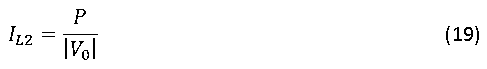
The power is given by:

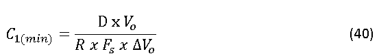
The minimum capacitance of the capacitors is given by:
Where,


Where ∆Vo is 1% to 5% of Vo
The SEPIC converter provides both step-up and step-down voltage conversion with continuous input and output currents. It maintains stable output voltage even when the input is close to or equal to the output, making it ideal for applications like automotive power supplies and battery chargers.
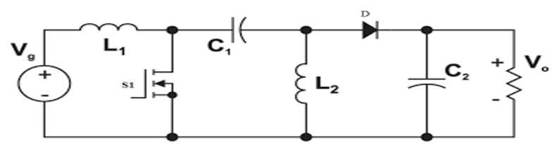
Figure 9: Diagram of a SEPIC converter
When switch S1 is closed, the current flows from the input voltage (Vg) through inductor L1, storing energy in its magnetic field and charging capacitor C1. When S1 opens, the collapsing magnetic field in L1 induces a voltage that adds to Vg, forward-biasing diode D and allowing current to flow to output capacitor C2 and the load. Energy from L1 and L2 charges C2. The output voltage (Vo) can be higher or lower than the input, depending on the duty cycle.
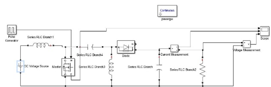
Figure 10: Circuit diagram of a SEPIC converter using MATLAB
The Duty cycle D is given as:
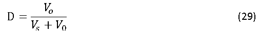
The minimum inductance of the inductors for the converter to work in continuous current mode is given by:
Where ∆IL1 is 20% to 40% of IL1
Where ∆IL2 is 20% to 40% of IL2
The power is given by:

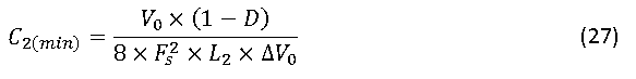
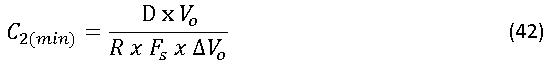
The minimum capacitance of the capacitors is given by:
Where ∆Vo is 1% to 5% of Vo

Where ∆Vo is 1% to 5% of Vo

This section presents the results obtained from the simulation of the DC-DC converter using MATLAB Simulink. The analysis and comparison between calculated values of the 3 DC-DC converters and the simulated result values for the purpose of knowing the differences in parameter values are given below.
4.1 Buck-Boost Converter A. Boost ModeValues of the components used in the analysis
Vs = 48V; R = 100 Ω; P = 100W; Fs = 10KHz; T = 0.0001s; Lactual= 656µH; Cactual = 16.9µF; Expected Vo = -100V.
Expected Vo = -100V.
Calculated result
D = 67.6%; ∆IL=4.95A; ∆Vo=5V; Vo = -100V; Io = -1A; IL(PP) = 4.95A; IL(P) = 5.57A; ILmin= 0.61A;
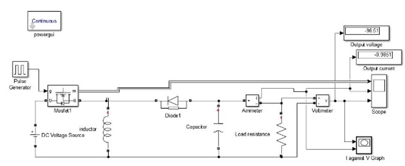
Figure 19: Circuit diagram of boost buck converter boost mode showing the output voltage and output current
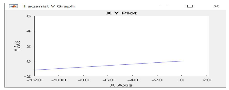
Figure 20: Boost buck converter boost mode graph of output current against output voltage
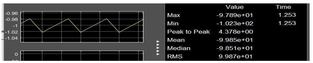
Figure 21: Boost buck converter boost mode capacitor ripple voltage graph
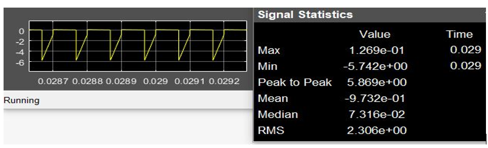
Figure 22: Boost buck converter boost mode inductor ripple current graph
Values of The Simulated ResultsVo = -98.51V
Io = -0.9851A
∆IL=I_max - Imin = 0.1269 -(- 5.742) = 5.87A
∆Vo=Vmax - Vmin = -97.89-(-102.3) = 4.38V
IL(PP) = 5.869A
IL(P) = -5.742A
ILmin= 0.1269A
Analysis from the calculated and simulated result of the buck-boost converter (boost mode) shows that the inductor current ripple has a difference of 0.924A, the output capacitor voltage ripple has a difference of 0.62V, the inductor peak to peak current has a difference of -0.919A, the inductor peak current has a difference of 0.172A, the inductor minimum current has a difference of 0.4861A, the output voltage has a difference of 1.49V, and the output current has a difference of 0.0149A.
B. Buck ModeValues of The Components Used in The Analysis
Vs = 48V; R = 100 Ω; P = 5.76W; Fs = 10KHz; T = 0.0001s; Lactual= 2.78mH; Cactual = 6.66µF; Expected Vo = -24V. Calculated Result
D = 33.3%; ∆IL=0.575A; ∆Vo=1.2V; Vo = -24V, Io = -0.24A; IL(PP) = 0.575A; IL(P) = 0.646A; ILmin= 0.072A;
Graphs and Results of Simulation
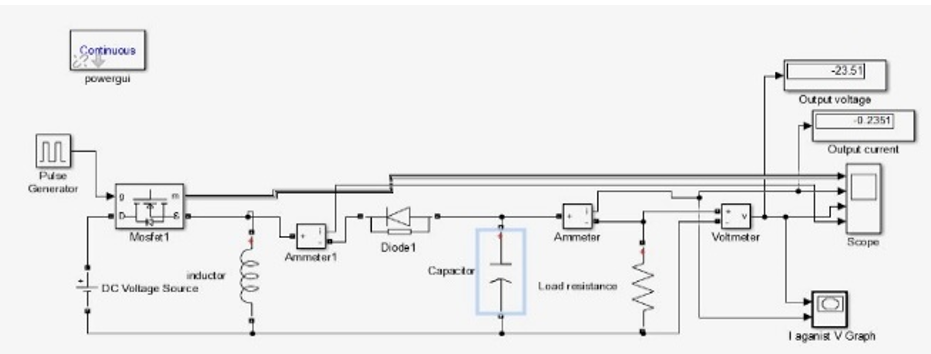
Figure 23: Circuit diagram of boost buck converter buck mode showing the output voltage and output current
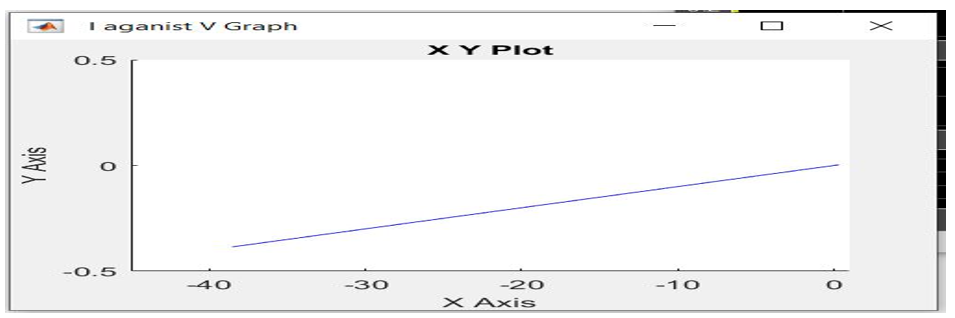
Figure 24: Boost buck converter buck mode graph of output current against output voltage
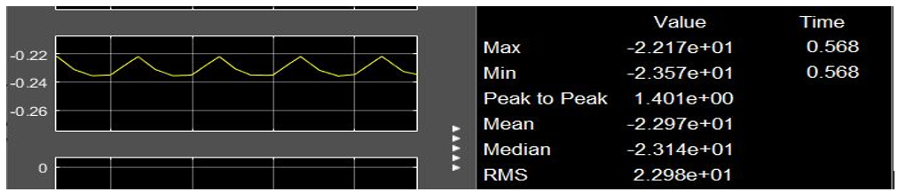
Figure 25: Boost buck converter buck mode capacitor ripple voltage graph
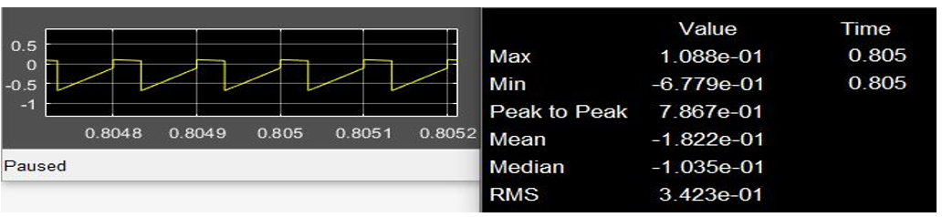
Figure 26: Boost buck converter buck mode inductor ripple current graph
Vo = -23.51V
Io =-0.2351A
∆IL=I_max - Imin = 0.1088 -(- 0.6779)= -0.7867A
∆Vo=Vmax - Vmin = -22.17-(-23.57) = 1.401V
IL(PP) = -0.7867A
IL(P) = -0.6779A
ILmin= 0.1088A
Graphs And Results of Simulation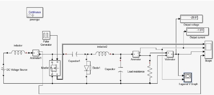
Figure 27: Circuit diagram of Ćuk converter showing the output voltage and output current
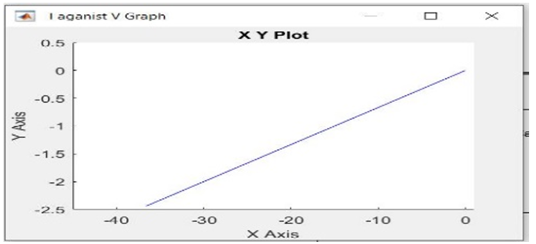
Figure 28: Ćuk converter graph of output current against output voltage
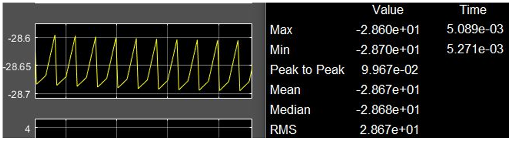
Figure 29: Ćuk converter output capacitor ripple voltage graph
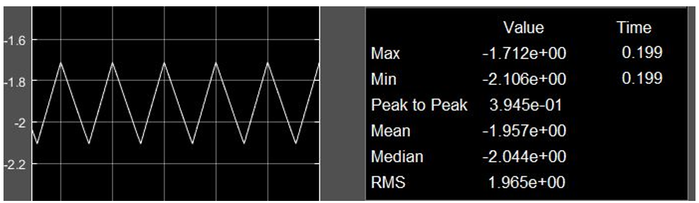
Figure 30: Ćuk converter inductor (L2) ripple current graph
Vo = -28.67V
Io =-1.911A
∆IL=I_max - Imin = -1.712 -(- 2.106) = 0.3945A
∆Vo=Vmax - Vmin = -28.6 -(-28.7) = 0.0997V
Analysis from the calculated and simulated result of the ćuk converter shows that the current ripple of inductor (L2) has a difference of 0.0055A, the output capacitor voltage ripple has a difference of 0.2003V, the output voltage has a difference of 1.33V, and the output current has a difference of 0.089A.
4.3 SEPIC Converter
Values of the Components Used in the Analysis
Vs = 15V; R = 2 Ω; P = 18W; Fs = 250KHz; T = 0.000004s; L1 = 35.62µH; L2 = 14.25µH; C1 = 28.57µF; C2 = 28.57µF; Expected Vo = 6V.
Calculated Result
D = 28.57%; ∆IL2=0.1.2A; ∆Vo=0.12V; Vo = 6V, Io = 3A
Graphs and Results of Simulation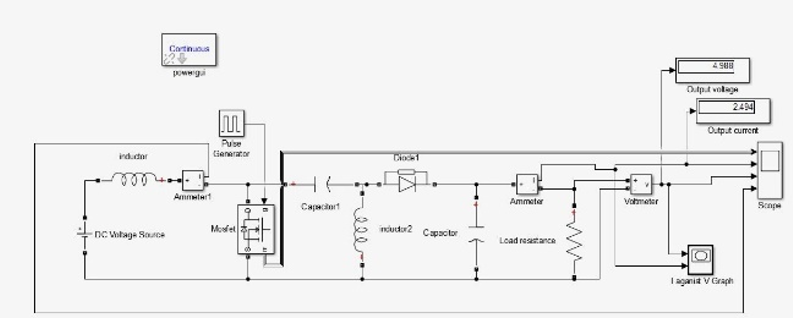
Figure 31: Circuit diagram of SEPIC converter showing the output voltage and output current
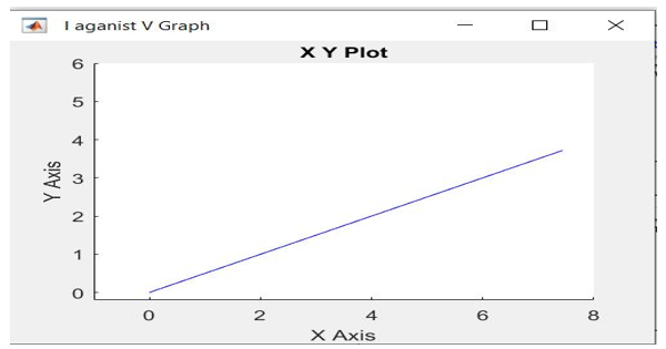
Figure 32: SEPIC converter graph of output current against output voltage
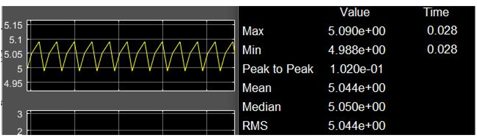
Figure 33: SEPIC converter output capacitor ripple voltage graph
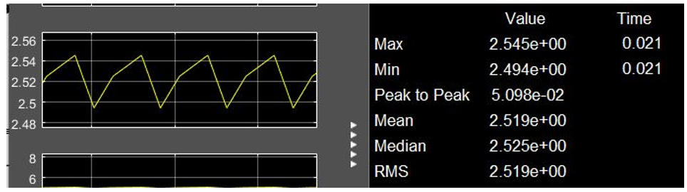
Figure 34: SEPIC converter inductor (L2) ripple current graph
Vo = 4.988V
Io =2.494A
∆IL=I_max - Imin = = 2.545-2.494 = 0.051A
∆Vo=Vmax - Vmin = 5.09-4.988 = 0.102V
Analysis from the calculated and simulated result of the sepic converter shows that the current ripple of inductor (L2) has a difference of 1.149A, the output capacitor voltage ripple has a difference of 0.018V, the output voltage has a difference of 1.012V, and the output current has a difference of 0.506A.
5. DISCUSSION AND CONCLUSIONThe simulation results demonstrate the converter’s ability to convert a given input voltage to the desired output voltage with minimal deviation from the theoretical values. This may be as a result of certain coded parameters of the components in the MATLAB software which were not accounted for in the theoretical calculations. But the simulated result values are within the acceptable range of 2 ± theoretical calculated values.
The primary aim of this project was to design and simulate various types of DC-DC converter, specifically, buck-boost, cuk and sepic converter using MATLAB simulink. Through a systematic approach, we explored their operational principles, designed their circuitry, and analyzed their performance including desired output voltage deviation, output current, voltage ripple and current ripple. The implementation of theoretical knowledge with practical simulation highlighted the significance of component selection. This entails that choosing the right values for inductors, capacitors, and switches was crucial for achieving desired performance.
In terms of future direction of this work, it has been said that Matlab/Simulink simulation software is employed for this modeling and simulation studies. Experimental verification of the control technique is hoped to be carried out through research visits with a view to supporting the analysis and simulation results so obtained.
DECLARATIONS:| Acknowledgments | : | Not applicable. |
| Conflict of Interest | : | The authors declares that there is no actual or potential conflict of interest about this article. |
| Consent to Publish | : | The authors agree to publish the paper in the Global Research Journal of Social Sciences and Management. |
| Ethical Approval | : | Not applicable. |
| Funding | : | Author claims no funding was received. |
| Author Contribution | : | Both the authors confirms their responsibility for the study, conception, design, data collection, and manuscript preparation. |
| Data Availability Statement | : | The data presented in this study are available upon request from the corresponding author. |
REFERENCES
- K. Bendaoud, K. Salah-ddine, J. Laassiri, L. Elmaimouni, “Modelling and simulation DC-DC power converter buck for mobile applications using MATLAB/Simulink,” International Journal of Intelligent Enterprise, Vol. 4, no. 1/2, January 2020.
- S. W. Shneen, D. H. Shaker and F. N. Abdullah, “Simulation model of PID for DC-DC converter by using MATLAB,” International Journal of Electrical and Computer Engineering (IJECE), vol. 11, no. 5, pp. 3791-3797,October 2021.
- M. S. Arifin and M. J. Alam, “Input switched closed-loop single phase SEPIC controlled rectifier with improved performances,” International Journal of Electrical and Computer Engineering (IJECE), vol. 11, no. 1, pp. 2088-8708, DOI: 10.11591/ijece.v11i1.pp1-8, February 2021.
- R. Salyam and V. Margaret, “Source-load-variable voltage regulated cascaded DC/DC converter for a DC microgrid system” International Journal of Electrical and Computer Engineering (IJECE), vol. 13, no. 1, pp. 2088-8708, DOI: 10.11591/ijece.v13i1.pp107-115, February 2023.
- A. H. Mary, A. H. Miry, M. H. Miry, “System uncertainties estimation based adaptive robust backstepping control for DC DC buck converter” International Journal of Electrical and Computer Engineering (IJECE), vol. 11, no. 1, pp. 2088-8708, DOI: 10.11591/ijece.v11i1.pp347-355, February 2021.
- E. Setiawan and I. Hodaka, “A Novel Nonlinear Control of Boost Converter using CCM Phase Plane,” International Journal of Electrical and Computer Engineering (IJECE), vol. 8, no. 6, pp. 4282 – 4289 ISSN: 2088-8708, December 2021.
- S. N. Rao, D. V. A. Kumar, C. S. Babu, “Grid Connected Distributed Generation System with High Voltage Gain Cascaded DC-DC Converter Fed Asymmetric Multilevel Inverter Topology,” International Journal of Electrical and Computer Engineering (IJECE), vol. 8, no. 6, pp. 4047-4059, ISSN: 2088-8708, December 2021.
- M. A. N. Kasiran, A. Ponniran, N. N. M. Siam, M. H. Yatim, N. A. C. Ibrahim and A. M. Yunos, “DC-DC converter with 50 kHz-500 kHz range of switching frequency for passive component volume reduction” International Journal of Electrical and Computer Engineering (IJECE), vol. 11, no. 2, pp. 1114-1122, ISSN: 2088-8708, DOI: 10.11591/ijece.v11i2.pp1114-1122, April 2021.
- S. Nallusamy and D. K. Rukmani, “Design and simulation of Arduino Nano controlled DC-DC converters for low and medium power applications” International Journal of Electrical and Computer Engineering (IJECE), vol. 13, no. 2, pp. 1400-1409 ISSN: 2088-8708, DOI: 10.11591/ijece.v13i2.pp1400-1409, April 2023.
- G. G. R. Sekhar and B. Banakara, “An Internal Current Controlled BLDC Motor Drive Supplied with PV Fed High Voltage Gain DC-DC Converter” International Journal of Electrical and Computer Engineering (IJECE), vol. 8, no. 2, pp. 1262~1272 ISSN: 2088-8708, April 2021.
- H. J. Motlak and A. S. Rahi, “Performance comparison of different control strategies for the regulation of DC-DC negative output super-lift luo-converter” International Journal of Electrical and Computer Engineering (IJECE), vol. 10, no. 6, pp. 5785-5792 ISSN: 2088-8708, DOI: 10.11591/ijece.v10i6.pp5785-5792, December 2020.
- E. Setiawan, T. Hirata and I. Hodaka, “Accurate Symbolic Steady State Modeling of Buck Converter” International Journal of Electrical and Computer Engineering (IJECE), vol. 7, no. 5, pp. 2374 – 2381 ISSN: 2088-8708, October 2021.
- M. N. Abdullah, M. K. M. Desa and M. N. Akhtar, “DC-DC Buck Converter for Electric Bike with Parameterized DC Motor: Simulation and Experimental Validation,” Journal of Physics: Conference Series DOI: 10.1088/1742-6596/2312/1/012059, August 2022.
- R. Palanisamy, K. Vijayakumar, V. Venkatachalam, R. Mano Narayanan, D. Saravanakumar and K. Saravanan, “Simulation of various DC-DC converters for photovoltaic system,” International Journal of Electrical and Computer Engineering (IJECE), vol. 9, no. 2, pp. 917-925, ISSN: 2088-8708, April 2021.
- Wikipedia, "MATLAB,"Wikipedia: The Free Encyclopedia , [Online]. Available: https://en.wikipedia.org/wiki/MATLAB. [Accessed: August 23, 2024].
Eterigho Okpomo Engr. Prof. Stephen Ejiofor Oti

lives at the Garden of Edem in UmuchagwuEdem-Ani in Nsukka Local Government Area of Enugu state of Nigeria. He received a B.Eng. (Electrical Engineering), an M.Eng. (Electrical Power Devices) and a Ph.D (Electrical Power Devices) degrees, all of the University of Nigeria in 1998, 2006 and 2014 respectively. He joined the Electrical Engineering Department, UNN as a Principal Technical Officer and was later in 2007 converted to the lecturing cadre in the same department. He is a member of Nigerian Society of Engineers (NSE). He is the current membership secretary of Nsukka Chapter of Nigerian Institute of Electrical and Electronic Engineering (NIEEE) and he is also a registered member of Council for the Regulation of Engineering in Nigeria (COREN). He has published several research articles both in local and international journals. His research areas include Machine modeling, Thermal modeling, Power and Energy systems modeling and Simulations.
Mr. Chinedu T. Obe
received a B.Eng. (Electrical Engineering) of University of Nigeria, Nsukka in 2014 and proceeded for the National Youth Service Corp. He thereafter enrolled for, and bagged the M.Eng. (Electrical Power Devices) degree, also of the University of Nigeria in 2018. His mind and eyes are presently focused on his Ph.D. work in South Africa. C.T. Obe joined the Electrical Engineering Department, UNN as a Technologist and was later in 2019 converted to the lecturing cadre in the same department. He has started publishing in reputable Journals.
Eze Cornelius Chinweotito
received the B.Eng degree in Electrical Engineering from University of Nigeria, Nsukka in 2025. Due to his passion for electronics especially power electronics he indulged in various researches and also building electronic-based projects. His current research interests include optimization of power supplies in electric vehicles, power electronics applications, microcontroller and IoT systems. He can be contacted at email: cornelius.eze.241975@unn.edu.ng WhatsApp: +2348165641505 . https://orcid.org/0009-0004-0116-4506).
Victory Chukwuemeka Madueme
obtained his Bachelors (B.Eng), Masters (M.Eng) and Doctorate (Ph.D) from the Department of Electrical Engineering, University of Nigeria Nsukka in 2012, 2015 and 2024 respectively. He is an academic staff of the same department specializing in Power systems, High Voltage Engineering and Renewable Energy Systems. His research interests are vast and not limited to Electrical Power Systems Economics, Power System Protection and Control using FACTS devices, Life Estimation of transformers, artificial neural network and AI techniques to analyze power systems, Renewable Energy System Technologies and Electrical Machines Modelling. He is a registered member of the Nigeria Society of Engineers (NSE - 2016), Nigeria Institute of Electrical and Electronic Engineers (NIEEE -2018) and the Council for the Regulation of Engineering in Nigeria (COREN - 2017). He can be contacted at email: victory.madueme@unn.edu.ng.
Engr. Ugbe, Oluchi Christiana
Christiana is a staff of the Department of Electrical Engineering at the University of Nigeria Nsukka, Enugu State, Nigeria. She holds a bachelor of Engineering (B.ENG) with Second Class Upper Division in Electrical and Electronic Engineering from Anambra State University, Uli, Anambra State, Nigeria, and a Master’s degree with Distinction in Computer and Electronic Engineering (Communication Option) from Nnamdi Azikiwe University, Awka, Anambra State. She is currently pursuing her Ph.D with African Center of Excellence for Sustainable Power and Energy Development (ACE-SPED). Her research interest includes communication, Automatic Control Systems and instrumentation, Machine Learning, Deep Learning, and Renewable Energy. She has authored and co-authored several publications with several renowned journals and publishers. Her ongoing research project includes; Optimization of the use of Renewable Energy for Rural Electrification, Renewable Energy Potential Estimation Using Climatic-Weather-Forecasting Machine Learning Algorithms, and Forecasting the potential of large-scale solar photovoltaic power generation inNigeria using deep neural networks. She is Currently a Training and Research Assistant with African Center of Excellence for Sustainable Power and Energy Development (ACE-SPED). You can reach her through oluchi.ugbe@unn.edu.ng
APPENDIXD = Duty cycle
Vs = Input voltage
Vo = Output voltage
L1(min) = Minimum inductance for first inductor
L2(min) = Minimum inductance for second inductor
L1 = Actual inductance of inductor for first inductor
L2 = Actual inductance of inductor for second inductor
IL1 = Current of first inductor
IL2 = Current of second inductor
∆IL1= Ripple current of first inductor
∆IL2 = Ripple current of second inductor
Vc = Capacitor voltage
Lmin = Minimum inductance
L = Actual inductance of inductor
IL = Inductor current
IL(peak to peak)= Inductor peak to peak current
IL(peak) = Inductor peak current
IL(min) = Inductor minimum current
∆IL= Inductor ripple current
Fs = Switching Frequency
Is = Input source current
P = Power
Io = Output current
R = Load resistance
C1min = minimum capacitance of first capacitor
C2min = minimum capacitance of second capacitor
∆Vc1 = Change in first capacitor ripple voltage
〖∆V〗o = Output or second capacitor ripple voltage
dVc1 = First capacitor ripple voltage
C1 = Actual capacitance of first capacitor
C2 = Actual capacitance of second capacitor
Cmin = minimum capacitance
∆Vo = Capacitor ripple voltage
Vc = Capacitor voltage